Applying Classroom Experience to Real-World Innovation

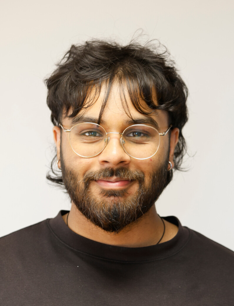
By Naveed Chowdhury, Junior Automotive Applications Engineer
As a Year in Industry (YINI) placement student with Diodes Incorporated (Diodes), I had the opportunity to work alongside professionals as an automotive applications engineer. YINI is a UK program that provides gap year opportunities for students focusing on the science, engineering, IT, and business disciplines. The aim is to help students like me get real-world experience and build my skill set.
I studied and specialised in Electronic Engineering at Manchester University (UK), so I saw this placement at Diodes as a direct fit to my studies. I have wanted to be an electronic engineer ever since I picked and prodded at my first computer, ever-curious as to what “magic” was making the computer work. This led me down a lifelong rabbit hole into the world of semiconductors and electronics in general.
This placement has been a perfect vehicle to ride in this world of semiconductors. Ever since the first day, I knew that working at a place like this aligned with my solid goal of becoming an engineer. It has fleshed out my knowledge by doing the engineering I have learnt at university and implementing the toolbox that the university provided me.
The work I’ve been carrying out during the placement has also developed that toolbox of skills, as I’m learning new things every day. For example, before the placement, I knew nothing about the world of electromagnetic interference (EMI) and electromagnetic compatibility (EMC), but now I’ve developed and proved my understanding through the creation of various application notes and PCBs. This placement has really shaped my fields of interest, and showed me where my strengths and areas of improvement are. Getting hands-on with teardowns, working with the Altium® designer, helping create the UK EMC lab, writing application notes, making various PCBs, and seeing the results of my work in the industry have all been valuable experiences in shaping me as an engineer.
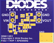
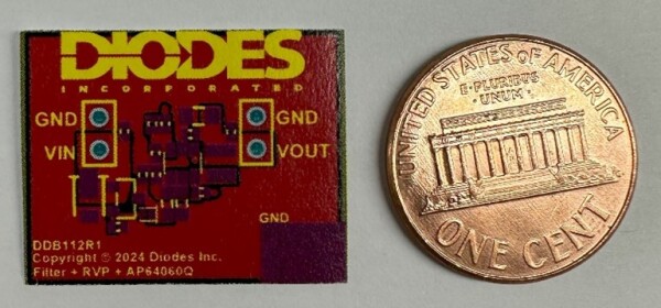
One of the highlights of my experience is also one of which I’m most proud of. I had the idea for a small form factor, low-cost DC-DC solution that meets emerging customer demands, and put the idea forward to my manager. Within just a couple of weeks, I designed a DC-DC converter PCB, the DDB112R1 (below), and it was sent to be manufactured. The device is ridiculously small; smaller than a one cent coin (20mm x 25mm to be exact)! This is a great example of the freedom I had to suggest new ideas and be creative, as any engineer should.
Figure 1. DDB112R1 PCB

Figure 2. DDB112R1 size comparison
Overall, I would say this placement has been a vital step in my career to really solidify my love and knowledge for engineering. If you’re an aspiring engineer, I would absolutely recommend seeking an placement in YINI to work at Diodes!
My next steps after this placement are to continue onto my 3rd year of university. During this, I anticipate gaining more vital knowledge and experience to increase my engineering toolbox. After university, I hope to gain the opportunity to work for Diodes again.
