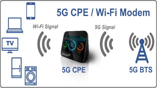

Our extensive families of PCIe Timing ICs are used by wireless industry leaders for high-performance products in the latest market applications.
We offer a large selection of PCIe ICs supporting generations 1.0 to 5.0 and that have two to twenty outputs, including:
● PCIe clock generators
● PCIe clock fanout buffers
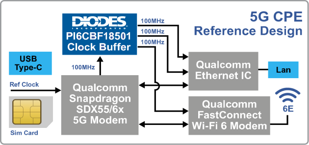
The PI6CBF18501 PCIe 4.0 fanout buffer used in this 5G CPE reference design supports a common-clock architecture that enables reliable high-speed chip-to-chip connections.
| PI6CBF18501 Key Features | Why PCIe Architecture? |
|
● 1.8V supply voltage ● Five outputs with on-chip termination ● Programmable slew rate and amplitude control ● Very low output jitter ● Industrial temperature range: ● -40ºC to 85ºC ● 5x5mm TQFN package |
● PCIe is the industry’s best supported, evolving, and scalable bus standard ● It features high-performance, power management, low BOM cost ● Qualcomm®-selected PCIe for chip-to-chip connections in mobile devices* |
Supports PCIe Standard Frequency 100MHz, Plus Other Frequencies from 25MHz to 250MHz
● Meets common PCIe requirements and enables alternate design options
Flexible Voltages Supported: 1.5V, 1.8V, 2.5V, 3.3V
● Easily interfaces to ICs with other voltages
On-Chip Termination: No Need for External Resistors
● Saves board space and reduces cost
Output Options: Two to Twenty Differential HCSL Outputs
● Supports very small to very large systems
Leading Supplier
● Diodes offer one of the industry’s largest selection of PCIe timing devices, from PCIe 1.0 to
PCIe 5.0, providing customers a wide choice of solutions
In addition to 5G CPEs, other PCIe applications include:
● Servers / Storage ● Industrial PCs ● Edge computing ● Networking ● Automotive