4V/3A, 6.7mΩ RON Switch with Adjustable Turn-On And Power Good
Log in or register to manage email notifications about changes to datasheets or PCNs for this part.
The AP22971 is a single-channel load switch with adjustable turn-on, an integrated power good (PG), and active output discharge path in an ultra-compact size.
The AP22971 contains an N-channel MOSFET that can operate over an input voltage range of 0.65V to 3.6V and switch currents up to 3A. An integrated charge pump biases the NMOS switch to achieve a minimum switch ON resistance (RON). The switch is controlled by an on-and-off input (ON), which is capable of interfacing directly with low-voltage control signals.
By default, the AP22971 has a fast turn-on time to minimize system startup and wait time. The adjustable slew rate can limit inrush current. A power good signal internally monitors the gate threshold and indicates when the switch is fully on.
The AP22971 includes thermal shutdown when the junction temperature is above the threshold, turning the switch off. The switch turns on again when the junction temperature stabilizes to a safe range.
The AP22971 has a 150Ω on-chip resistor for quick discharge of the output when the switch is disabled to avoid any unknown states caused by a floating supply to the downstream load.
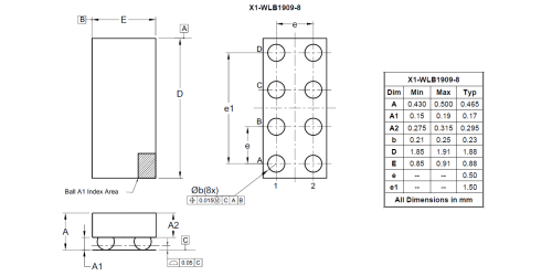
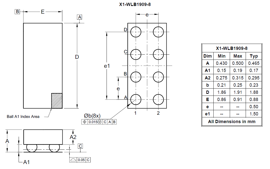
The AP22971 is available in the ultra-small X1-WLB1909-8 package.
Type |
Load Switch |
|---|---|
Compliance (Only Automotive Supports PPAP) |
Standard |
Quiescent Current Typ (μA) |
30 |
Maximum Continuous Output Current (A) |
3 |
Channels |
1 |
Enable Logic |
Active High |
Minimum Operating Voltage (V) |
0.65 |
Maximum Operating Voltage (V) |
3.6 |
RDS(ON) (VIN = 5V) Typ (mΩ) |
6.7 |
Reverse Current Block |
No |
Output Discharge |
Yes |
(TYP) Output Rise Time mS |
1.23 |
Power Good |
Yes |
UL Certificate |
No |
Something went wrong with your request. Please try again later. If this problem continues, please contact Diodes support for assistance.
A PCN may only apply to specific orderable part numbers in this datasheet. Please refer to the corresponding PCN to see the exact orderable part number(s) affected.
| PCN # | Issue Date | Implementation Date | Subject |
|---|---|---|---|
| PCN-2770 | 2025-10-30 | 2025-10-30 | Add Fab Site Code, Country of Diffusion (COD) and Assembly Site Origin (ASO) on Product and Shipping Labels for all Diodes Products |
